

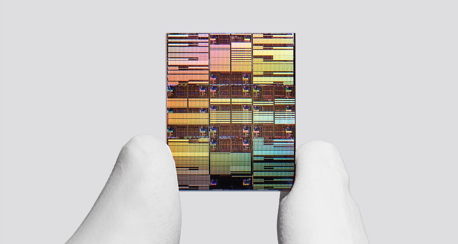
IBM this week claimed the first sub-nanometre chip, a era it calls the 0.7nm, or 7-angstrom, node. It says the design packs almost 100 billion transistors onto a fingernail-sized floor, about twice the density of its 2nm chip from 2021, with as much as 50% extra efficiency or 70% higher power effectivity. Manufacturing may start inside 5 years.
“This is a vital engineering milestone,” mentioned Francesco Petruccione, director of the Nationwide Institute for Theoretical and Computational Sciences (NITheCS) and professor of quantum computing at Stellenbosch College. “It reveals that chip producers are nonetheless discovering methods to make laptop chips extra highly effective and extra energy-efficient, regardless of many specialists believing that conventional scaling was approaching its limits.”
For many years, chips improved by shrinking transistors and packing extra facet by facet on a flat sheet of silicon. That method is hitting the bounds of physics. IBM’s reply, a design it calls “nanostack”, stacks transistors on high of each other, like flats in a tower block relatively than homes unfold throughout open veld, so the identical footprint can now maintain much more.
IBM has described the redesign, not the shrinking, as the true story. “We’re not simply making smaller transistors; we’re reinventing how chips are constructed,” mentioned IBM Analysis director Jay Gambetta.
Petruccione agreed that’s the crux: “The true innovation shouldn’t be merely making transistors smaller, however redesigning how they’re organized in three dimensions, opening a brand new path for future generations of computing {hardware}.” Labels like “2nm” and “0.7nm” are names for a era of know-how, not the literal width of a transistor.
For scale, at present’s finest laptop computer processor, Apple’s M3 Max, has about 92 billion transistors throughout the entire chip; IBM suits a comparable quantity onto a single fingernail. Chip makers spend such a achieve on extra pace or decrease energy, and Petruccione expects each to succeed in customers.
The affect
“For customers, it may finally translate into quicker smartphones and laptops, longer battery life and extra succesful AI assistants working immediately on gadgets,” he mentioned. “For companies, the larger affect is more likely to be decrease power prices in information centres and the power to course of a lot bigger AI workloads, making superior AI purposes extra inexpensive and broadly out there.”
Higher chips go to the center of the AI growth. “AI progress more and more relies upon not solely on higher algorithms but in addition on higher {hardware},” Petruccione mentioned. “Coaching and working trendy AI fashions require monumental quantities of computational energy and electrical energy. Extra environment friendly chips permit us to carry out extra AI computations utilizing much less power … advances in semiconductor know-how are subsequently changing into simply as essential as advances in AI software program.”
A second milestone is aimed much more squarely at AI. Alongside the transistor depend, IBM reported a roughly 40% enchancment in on-chip SRAM, the quick reminiscence beside the processor. Trendy AI fashions are sometimes held again much less by uncooked compute than by the power and time spent shuttling information to and from separate reminiscence chips; denser on-chip reminiscence retains extra of it subsequent to the engine doing the work, easing that bottleneck.
Chip vs mind
So, how a lot nearer does this take us to the human mind? In uncooked scale, a bit of, however lower than the headlines counsel. The mind’s estimated 86 billion neurons put IBM’s 100 billion transistors in the identical ballpark, however the mind’s actual unit of connection is the synapse, and it has on the order of 100 trillion of them, round a thousand occasions the chip’s transistor depend. Doubling density over the sooner 2nm chip solely halves the silicon wanted to shut that hole; you’d nonetheless want roughly a thousand of those fingernail-sized clusters wired collectively to match the mind’s connections.
Learn: Honey, I shrunk the chips – inside TSMC’s 2nm breakthrough
And matching the mind’s scale shouldn’t be the identical as matching the mind. A transistor is an easy on-off change, whereas a synapse is a residing connection that consistently rewires itself. For AI, the gap is shorter: a mannequin’s “dimension” is commonly measured in parameters, which loosely do the job synapses do, and the largest now run into the trillions. GPT-4 was broadly reported at round 1.8 trillion, with later fashions thought bigger nonetheless, leaving main fashions maybe 10 to 50 occasions in need of the mind’s synapse depend relatively than a thousand-fold. Chips like this one don’t shut that hole a lot as make the fashions cheaper and fewer power-hungry to run, the sensible approach the brand new {hardware} nudges AI ahead.
What South Africa ought to take from it
South Africa is not going to be making modern chips, however Petruccione argues that’s not the place the chance lies. “We are able to construct experience in designing AI algorithms, creating software program, quantum computing, quantum applied sciences and high-performance computing,” he mentioned. “Future competitiveness will more and more rely upon investing in superior digital abilities, analysis and human capital. International locations that put together their workforce for this new period will likely be much better positioned to profit from the following wave of technological innovation.”
IBM has proven “a powerful analysis prototype, however there’s nonetheless a major hole between a laboratory demonstration and high-volume industrial manufacturing”, he mentioned. The five-year timeline is “believable, however in all probability many engineering and financial challenges stay”. — © 2026 NewsCentral Media

